


| Chungbuk National University Team Decodes Growth Process of Plasma-Assisted Epitaxial Silicon | |||||||||||||||
| Writer | 관리자 | ||||||||||||||
|---|---|---|---|---|---|---|---|---|---|---|---|---|---|---|---|
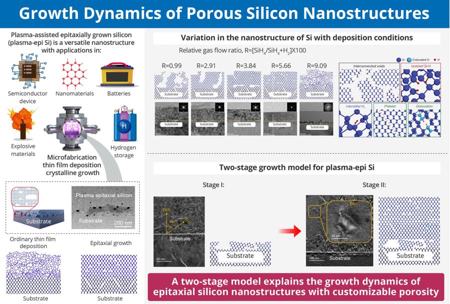
Image title: Uncovering the growth dynamics of defective nanostructures of plasma-epi Si Image caption: Scientists have elucidated the two-stage growth process of epitaxially grown plasma-epi Si and proposed strategies to customize nanostructure defects for desired properties. Image credit: Ka-Hyun Kim from Chungbuk National University License type: Original Content Usage restrictions: Cannot be reused without permission
Plasma-assisted epitaxy can grow single-crystal silicon (plasma-epi Si) at low temperature of 200 °C, whereas conventional single-crystal silicon is grown by the Czochralski method at approximately 1500 °C. However, plasma-epi Si usually shows undesirable electrical properties. Researchers from Korea have now explored the growth dynamics of plasma-epi Si to reveal a two-stage evolution. They also propose strategies to tailor the nanostructure for various applications, ranging from electronic devices, gas sensors, and lithium-ion batteries. The fabrication of microelectronic components of widely used electronic devices involves several thin-film deposition processes. One of them is epitaxy, which can be used to grow thin crystalline films with a specific crystal structure and direction. When silicon (Si) is grown epitaxially using plasma-assisted chemical vapor deposition (denoted as plasma-epi Si) a new material with a customizable nanostructure is obtained.
Although plasma-epi Si is a novel material, it has not garnered much scientific attention due to unsuitable electrical properties. However, since the nanostructure of plasma-epi Si can be easily manipulated, it can be used in various applications. In particular, nanometer-scale voids can be introduced, with control over both the quantity and arrangement.
In a new study published in Small Structures on 19 December 2023, Associate Professor Ka-Hyun Kim from Chungbuk National University and his team of researchers have investigated the growth dynamics of plasma-epi Si grown under various process conditions. “This research provides general knowledge on the defect nanostructure in crystalline silicon. In a departure from the conventional approach, we present a study on the hydrogen-incorporated nanostructure of plasma-epi Si and its growth dynamics, correlating the hydrogen incorporation with the defect nanostructure of the material,” explains Prof. Kim. In the study, the nanostructure of the plasma-epi Si was manipulated by exploring different deposition conditions to grow films of different nanostructures. One of the examined conditions involved altering the relative flow ratio of the constituent gases, which influenced the concentration of atomic hydrogen. Theoretical simulations were conducted to support the experimental results. The experimental observations of the study revealed a two-stage evolution of the nanostructure, characterized by different dominant nanostructure defects. In the initial stage, the nanostructure can be manipulated via the deposition conditions, resulting in a porous and interconnected structure that is dominated by voids, because of high hydrogen incorporation. In the subsequent bulk growth stage, the material growth is less sensitive to the deposition conditions, but evolves with film thickness, leading to the prevalence of isolated defects in the evolving nanostructure. Based on these findings, the researchers propose distinct deposition strategies for different applications. To enhance carrier transport properties in electronic applications, it is recommended to suppress strain during the initial growth stage, alongside controlling isolated bulk defects. On the other hand, for applications involving bottom-up-grown Si, a consistent supply of strain during growth is suggested.
“Crystalline Si is a material widely used in the semiconductor and solar industries. Through this development of bottom-up-grown plasma-epi Si, we can expand the application of crystalline Si into various fields such as gas sensors, lithium-ion batteries, hydrogen storage, and even explosives,” envisions Prof. Kim.
In summary, these findings elucidate the growth dynamics of plasma-epi Si, a new Si-based material with a customizable nanostructure and porosity. Additionally, the researchers have suggested different strategies for optimizing the plasma-epi Si growth process tailored to specific applications. These results thus contribute to a deeper understanding of this material and pave the way for the identification of diverse applications for bottom-up-grown porous Si!
Reference
About the institute Chungbuk National University (CBNU) is one of the ten Flagship Korean National Universities, a term for institutions in South Korea united under the "Presidential Council of the Korean Flagship National Universities." Since its establishment on September 27, 1951, Chungbuk National University has grown to include 13 Colleges and 8 Graduate Schools. In 1999, CBNU achieved recognition as part of the Brain Korea 21 Initiative by the Ministry of Education. Additionally, in 2003, the university was honored as the top institution in the project fostering regional universities by the Ministry.
Website: https://www.cbnu.ac.kr/site/english/sub.do?key=1427
About the author Prof. Ka-Hyun Kim is an Associate Professor at the Department of Physics at Chungbuk National University. The primary research topics of his group include thin-film deposition, material properties of low-temperature-grown epitaxial silicon, and the device physics of various semiconductor devices, with a particular focus on crystalline silicon solar cells. Before joining Chungbuk National University, he served as a senior researcher at the Korea Institute of Energy Research. In 2012, Ka-Hyun Kim earned a Ph.D. in Physics from Ecole Polytechnique, France.
|
|||||||||||||||
| Attachments | |||||||||||||||