


| NANO CONVERGENCE OPTOELECTRONICS LAB | |
  NANO CONVERGENCE OPTOELECTRONICS LAB The Nano Convergence Optoelectronics Lab (NCOL) engages in the exploration of nanoscale physics resulting from the hybridization of diverse nanomaterials for applications in electronics and optoelectronics. Research within the lab focuses on hybrid systems involving two-dimensional materials like graphene, MoS2 , and hBN, combined with low-dimensional nanomaterials, such as quantum dots and nanowires. The aim is to investigate novel physics at the nanoscale, paving the way for the development of innovative functionalities and next-generation devices. The lab also investigates novel materials and new processes aimed at overcoming physical limitations and addressing technical issues in CMOS semiconductor technology.
PROGRESS AND ACHIEVEMENTS The NCOL is actively engaged in researching novel physics and material science across a range of low-dimensional materials at the nanoscale. This involves exploring optical and electrical properties, as well as examining the effects of defects, doping, additives, junctions, interfaces, and novel functionalities for device applications. The investigation is facilitated through the utilization of optical and electrical characterization equipment, including micro-PL/Raman spectroscopy combined with a low-temperature magneto cryostat and electrical characterization instruments. Furthermore, the lab is equipped with thin film deposition tools, photolithography equipment, and plasma etching systems, enabling the semiconductor device fabrication process.
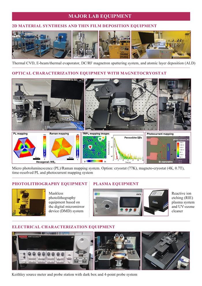
MAJOR RESEARCH ACCOMPLISHMENTS Polymer-waveguides-integrated 2D semiconductor heterostructures for optical communications. Nano Letters, DOI: 10.1021/acs.nanolett.3c03317 Increased mobility and reduced hysteresis of MoS2 field-effect transistors via direct surface precipitation of CsPbBr3 -nanoclusters for charge transfer doping, Nano Letters, DOI: 10.1021/acs.nanolett.3c02293 Switchable, tunable, and directable exciton funneling in periodically wrinkled WS2 , Nano Letters, DOI: 10.1021/acs.nanolett.0c02619 Comparative analysis of Schottky barriers for heterogeneous defect domains in monolayer WS2 field-effect transistors, Applied Surface Science, DOI: 10.1016/j.apsusc.2022.154600 Growth mode control of CVD-grown WS2 monolayer flakes via O2 pre-annealing for organic surfactant oxidation, Applied Surface Science, DOI: 10.1016/j.apsusc.2022.152564 Organic anisotropic excitonic optical nanoantennas, Advanced Science,DOI: 10.1002/advs.202201907 Tip-induced nano-engineering of strain, bandgap, and exciton dynamics in 2D semiconductors, Advanced Materials, DOI: 10.1002/adma.202008234 MAJOR LAB EQUIPMENT 2D MATERIAL SYNTHESIS AND THIN FILM DEPOSITION EQUIPMENT Thermal CVD, E-beam/thermal evaporator, DC/RF magnetron sputtering system, and atomic layer deposition (ALD) OPTICAL CHARACTERIZATION EQUIPMENT WITH MAGNETOCRYOSTA Micro photoluminescence (PL)/Raman mapping system. Option: cryostat (77K), magneto-cryostat (4K, 0.7T), time-resolved PL and photocurrent mapping system PHOTOLITHOGRAPHY EQUIPMENT Maskless photolithography equipment based on the digital micromirror device (DMD) system PLASMA EQUIPMENT Reactive ion etching (RIE) plasma system and UV-ozone cleaner ELECTRICAL CHARACTERIZATION EQUIPMENT Keithley source meter and probe station with dark box and 4-point probe system
|